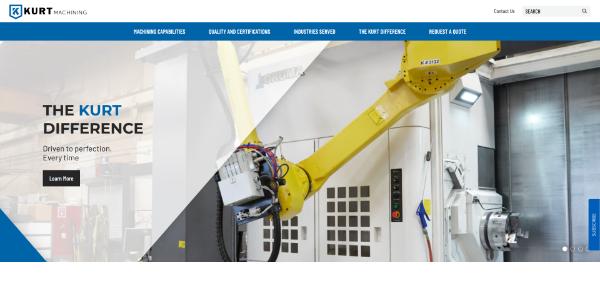
What Is Microfabrication?
While the term is not strictly defined, "microfabrication" is generally used to refer to technologies for performing fabrication at the micron or nanometer scale, or for performing fabrication on micron- or nanometer-scale objects.
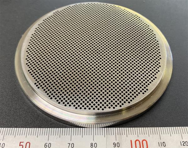
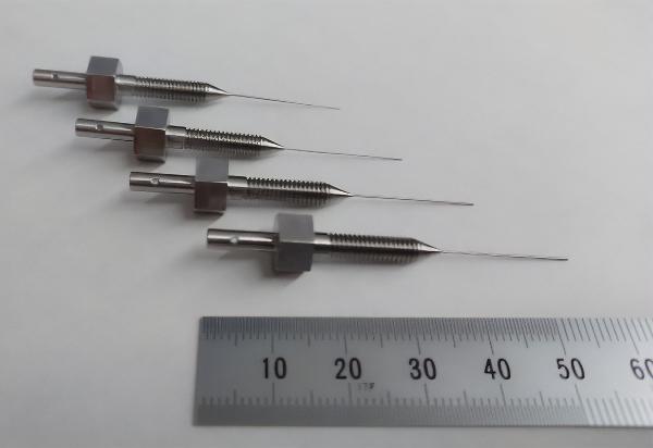
Fabrication is done at a scale that is invisible to the naked eye using equipment and methods such as CNC devices, lasers, and chemical treatment.
This technology is vital for fields requiring high levels of precision, such as the semiconductor,electronic device, or medical device fields.
Main Types of Microfabrication
A variety of techniques are used to perform microfabrication, and each fabrication method is different.
Below are some of the most typical fabrication methods.
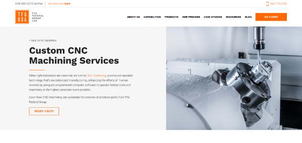
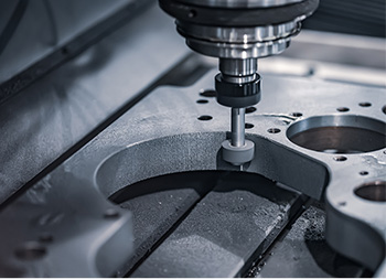
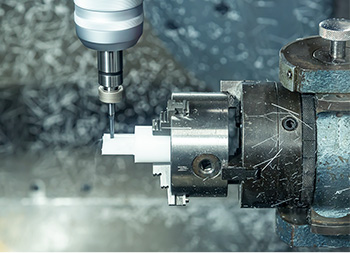
- Milling: Precision blades are used to cut material from the target object. This fabrication technique is also used when working with difficult-to-cut materials.
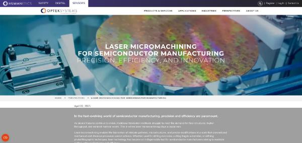
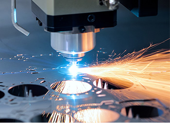
- Laser processing: Lasers are used to melt and evaporate material from the target object.
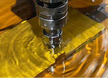
- Electrical discharge machining: Electricity is discharged between an electrode and the target object, and the resulting heat melts material from the object.
- Photolithography: Light irradiation is used to form precise patterns on the target object.
This is a core technology used in creating micrometer-sized components and performing surface processing.
- Etching: Chemicals are used to dissolve material from the surface of the target object and create complex shapes.
Main application fields
- Semiconductor
- Aerospace
- Biomedicine
- Electronics
- MEMS
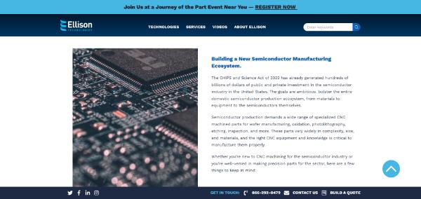
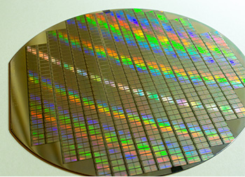
Microfabrication in the Semiconductor Field
Microfabrication is an important technology for semiconductor manufacturing.
Every year,semiconductors are becoming more and more miniaturized, requiring nanometer- and angstrom-level precision.
Microfabrication is expected to continue to play an important role, supporting the ultra-high precision fabrication of these devices.
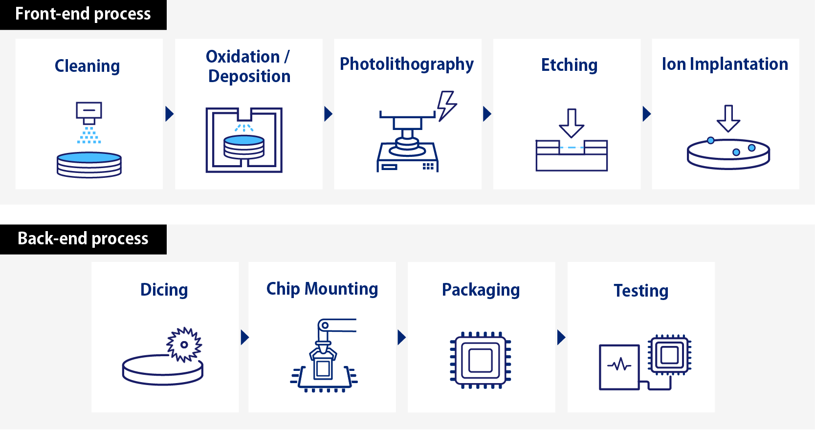
Semiconductor Manufacturing Processes
▼Scrollable
Semiconductor manufacturing can be broadly divided into two phases: upstream and downstream.
During upstream processing, microfabrication technologies such as photolithography or etching are used to form circuit patterns on wafers. These processes are repeated dozens of times to create laminated structures.
Microfabrication is primarily used during these upstream processes.
During the downstream processes, the semiconductors are finished off.These processes include mounting and testing chips, packaging, and the like.
There is a great deal of division of labor in the semiconductor industry, so upstream processes and downstream processes are usually contracted out to different companies.