Potomac
Open Table of ContentsClose Table of Contents
Source: Potomac's Official Website (https://www.potomac-laser.com/)
Potomac provides integrated support, from prototyping to mass production, through its microfabrication services, which center around its laser processing services.
This page introduces its microfabrication features, the processing services it offers, processing examples, and more.
Potomac's microfabrication services
Potomac has been supplying laser microfabrication services since it was founded in 1982.
It uses multiple lasers with different bandwidths (193 nm to 10,600 nm) depending on the materials to be processed and how the finished articles will be used. This laser processing is highly precise and has minimal thermal impact.
It handles both prototyping and mass production with the same equipment, so scaling up is easy.
Fabrication services
Potomac's microfabrication services are primarily focused on contactless processing using lasers.
Its processing capabilities include cutting, drilling, marking, surface patterning, welding, and more.
It also has 3D printing and hot embossing for forming three-dimensional structures on base materials after laser processing, along with technologies for bonding and assembling components.
Potomac can handle the entire process of creating a completed device through its integrated system.
Supported materials
Potomac's laser microfabrication services support a wide selection of materials, and it can precisely process complex shapes on everything from thin films to tubular materials through its multi-axis transport system.
Material supplier Goodfellow is part of the same group, so Potomac's integrated proposals extend from material selection to processing.
Supported sizes
Not listed on the company website.
CHECK Finding Your Partner Based on Processing Style
One of Potomac's strengths is its range of multi-wavelength lasers, so the right wavelengths can be chosen based on the optical absorption properties and thermal impacts of individual materials.
Another feature is that it has supplementary in-house technologies such as micro CNC machining, hot embossing, and micro 3D printing technologies.
It makes a great partner for companies who want to holistically consider processing methods and equipment with an eye toward the transition from the prototyping stage to the mass production stage.
This site recommends various microfabrication service providers for companies searching for microfabrication partners.
Examples of Potomac's microfabrication
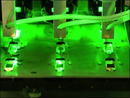
Scaling up copper substrates with high aspect ratio channels from prototyping to mass production
Source: Potomac's Official Website (https://www.potomac-laser.com/about/case-studies/laser-micromachining-ramp-up-of-complex-semiconductor-part/)
Potomac designed and built a high power laser system with multiple beams to shorten the processing time for a project, which took roughly 5 hours during the prototyping stage, to just 3 minutes and 17 seconds per part.
The project was a difficult one requiring a high level of shape precision and edge quality in minute channels formed on a copper substrate.
By optimizing the equipment design, Potomac was able to ramp up from prototype verification to mass production in a short period of time.
* Source: Potomac's Website (https://www.potomac-laser.com/about/case-studies/laser-micromachining-ramp-up-of-complex-semiconductor-part/)
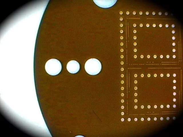
Completing processing using 21 different microhole patterns
in less than a week
Source: Potomac's Official Website (https://www.potomac-laser.com/about/case-studies/microhole-drilling-services/)
In this case example of a project for an electronics company, Potomac was able to perform drilling using patterns containing numerous microholes, between 10 µm and 200 µm, in Kapton (polyimide) and Mylar (polyester) material with a short turnaround time.
The number of microholes per part varied between 50 and 10,000, and critical tolerances included hole diameter, positioning, and taper, yet all designs were completed in under a week.
* Source: Potomac's Official Website (https://www.potomac-laser.com/about/case-studies/microhole-drilling-services/)
Company Information
| Company Name |
Potomac Photonics, Inc. |
| Location |
1450 South Rolling Road
Baltimore, MD 21227
USA |
| Telephone |
+1-(443)-543-5737 |
| Website |
https://www.potomac-laser.com/ |