This page presents the features of companies that offer photolithography services.
Eulitha
Eulitha provides photolithography services for creating high-resolution, nanoscale structures. It uses electron beam lithography (EBL) and laser interference lithography (LIL) to create custom patterns with up to 50 nm resolutions on substrates made out of materials such as silicon or quartz.
It handles everything from mask design to exposure and pattern property evaluation, supporting research and development in the optical, semiconductor, and bio-device fields.
Company Information
Company Name
Eulitha AG
Location
Headquarters: Grosszelgstrasse 21
5436 Würenlos
Switzerland
USA Office: Eulitha US, Inc.
8561 154th Avenue NE, Suite 100
Redmond, Washington 98052
USA
Telephone
Headquarters: +41 56 281 21 52
USA Office: +1-(425)-236-0795
MSE Supplies specializes in custom photolithography for research and prototyping purposes. With its 365 nm UV photolithography equipment it can create fine patterns, as small as 5 µm, with high precision.
It uses liftoff and wet etching methods and works with diverse materials, such as glass, silicon, and flexible substrates. It performs its manufacturing in a cleanroom environment, and its services are used for the development of prototype MEMS devices, chemical and bio-sensors, and micro-electrodes.
Company Information
Company Name
MSE Supplies LLC
Location
2705 East Medina Road, Suite 161
Tucson, AZ 85756
USA
Cirtec Medical's strengths lie in its microfabrication technologies for medical devices. It uses proprietary additive photolithography processes to create high-density conductive traces with resolutions of 1 to 2 µm.
It maintains uniform precision even across substrates with large surface areas, measuring up to 12 inches by 12 inches. Its patterning is highly suited for thin-film multilayer circuits and flexible substrates. It has established a solid reputation in the micro-electronic circuit manufacturing field for its bio-sensors and wearable medical devices.
Company Information
Company Name
Cirtec Medical Corporation
Location
9200 Xylon Avenue North
Brooklyn Park, Minnesota 55445
USA
Alfa Chemistry supplies photolithography services for fields such as the semiconductor and MEMS fields. Its electron beam lithography (EBL) has a resolution of 10 nm, its stepper lithography has a resolution of 0.35 µm, and its contact and proximity lithography has a resolution of 1 µm.
It uses 365 nm UV photolithography equipment to form minute patterns on diverse substrates, including glass and silicon substrates. It combines metal liftoff and wet etching processes to handle everything from photoresist removal to pattern transfer.
Advance supplies high-precision photolithography and photomasking services. It can create patterns at the submicron level and has the technological capabilities to handle even complex designs.
Using its unique photolithography techniques, it can perform high precision processing with short turnaround times. It performs custom work based on requests from process engineers and research organizations and supplies innovative solutions for the photolithography field.
Company Information
Company Name
Advance Reproductions
Location
100 Flagship Drive
North Andover, Massachusetts 01845
USA
Silicon Valley Microelectronics supplies photolithography and patterning services for semiconductor wafers. It works with silicon and glass substrates measuring from 50 to 300 mm and uses diverse photolithography techniques such as immersion, scanning, stepper processing, contact and proximity alignment, and electron beam lithography.
It performs microfabrication for 65 nm to 250 nm nodes and supports standard patterns and custom designs for process evaluations such as CMP, TSV, and WLP.
Reynard Corporation is known for its manufacturing of pattern photochemical thin film by combining optical thin film coating and photolithography technologies. It can form patterns as small as 5 µm on substrates measuring up to 18 inches and has a track record of multilayer stacking and alignment with a precision of 25 µm or less.
Its primary products are optical filters, reticles, beam splitters and other devices that improve the functionality of optical devices and sensors. Its services are also used in the semiconductor field for exposure-related components.
Company Information
Company Name
Reynard Corporation
Location
1020 Calle Sombra
San Clemente, California 92673
USA
Teledyne focuses on micro-pattern formation using photolithography. It uses ASML PAS 5500/60B i-line steppers and contact aligners to perform high-precision photolithography of patterns with resolutions as small as 0.45 µm on 3- to 8-inch wafers. In addition to silicon, it also works with glass and multi-layer film.
It supports both positive and negative photoresists and thick film SU-8, assisting with the precision processing involved in MEMS device manufacturing.
Company Information
Company Name
Teledyne MEMS (Teledyne DALSA division)
Location
Edmonton Foundry: 1911-94 Street
Edmonton, Alberta T6N 1E6
Canada
Bromont Foundry: 18 Boulevard de l'Aéroport
Bromont, Québec J2L 1S7
Canada
First, it's vital to focus on the potential partner's technical capabilities, such as the resolutions and substrate sizes it supports, along with its equipment environment and quality. Even high-resolution equipment can produce finished articles with pattern defects caused by particle interference if processing is performed in an environment other than a cleanroom.
Processing limits vary depending on the wavelengths of the light sources and the types of resist, so it's best to pick a company whose exposure methods match your resolution needs. You'll also want to check the company's prototyping capabilities and its delivery time flexibility.
[Choose by Fabrication Type] Top Three Recommended Microfabrication Partners
For difficult-to-cut materials
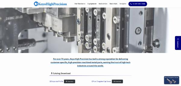
Koyo High Precision
Source: Koyo High Precision website (https://koyohighprecision.com/)
Examples of supported materials
Tungsten, molybdenum, tantalum,etc.
Main fabrication technologies
Micro drilling
Lathe machining
Milling
Why We Recommend
They perform fabrication for a wide range of sizes, from ⌀3 to 220 mm,and they can handle everything from prototype development to mass production fabrication for difficult-to-cut materials
They can achieve a fabrication precision of ±3 μm even for tungsten,which is known for being difficult to cut.