OpTek Systems
Open Table of ContentsClose Table of Contents
Source: OpTek Systems's Official Website (https://www.humaneticsgroup.com/sensors)
OpTek Systems is a global enterprise that possesses various technologies for performing high-precision microfabrication using industrial lasers and for performing optic fiber processing.
It supplies its high-precision laser processing services and production facilities to a wide range of fields, including the semiconductor, photoelectronic, medical device, and energy fields.
This page introduces the features of OpTek Systems' microfabrication, the processing services it offers, processing examples, and more.
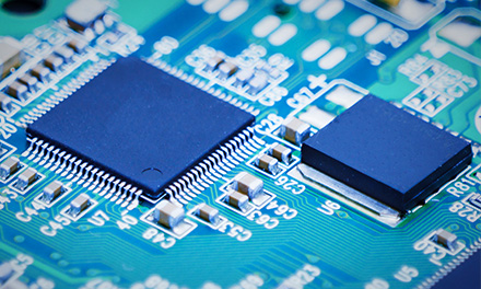
OpTek Systems' microfabrication services
One of OpTek Systems' strengths is that it uses laser with a wide range of wavelengths, from ultraviolet (UV) to infrared (IR), optimizing its process conditions based on the characteristics of the material to be processed and the requirements of the shapes to be created.
Its contactless laser processing enables it to create microstructures at the micron and sub-micron level, something that is difficult to accomplish with conventional machining.
It achieves extraordinarily high dimensional precision, with a tolerance of ±0.001 mm or less.
With process service sites in both the US and the UK, it can handle orders for everything from prototyping to mass production.
Fabrication services
OpTek Systems uses contactless lasers with zero tool wear. It combines a variety of processing modes to provide microfabrication services such as drilling, multi-layer structure cutting, groove and line formation, conductive pattern and insulating pattern creation, semiconductor wafer splitting, and ceramic substrate splitting.
Supported materials
OpTek Systems works with the main materials used in semiconductor manufacturing and electronic component processing, such as metal, ceramic, plastic, and glass.
It selects laser wavelengths and optimizes output conditions based on the absorption properties of materials, and it maintains stable processing quality, preventing cracking even in brittle materials.
Supported sizes
OpTek Systems can perform laser drilling with diameters ranging from several µm to several hundred µm.
Furthermore, it maintains the same high level of precision for laser scribes a few tens of µm wide and several kilometers long. It achieves consistent edge shape precision and reproducibility even for microscopic shapes and produces uniform openings.
It is the perfect partner for applications requiring extremely fine dimensional precision, such as optical devices and semiconductor structures.
CHECK Finding Your Partner Based on Processing Style
One of the things that sets OpTek Systems apart is that its contactless processing, performed using lasers with a wide range of wavelengths, produces fine, high-precision structures while preventing the effects of heat.
It works with all kinds of materials, from metal to ceramic and glass, so it is perfect for fields such as the semiconductor, optical device, and medical device fields which require fine-dimension fabrication and high quality.
In addition to OpTek Systems, this site presents other microfabrication service providers, categorized by fabrication method. Use it to help find the fabrication partner that's right for you.
Examples of OpTek Systems' microfabrication
Not listed on the company website
Company Information
| Company Name |
OpTek Systems, Inc. |
| Location |
23300 Haggerty Road
Farmington Hills, MI 48335
USA |
| Telephone |
+1-(248)-778-2000 |
| Website |
https://www.humaneticsgroup.com/ |