WOP
Open Table of ContentsClose Table of Contents
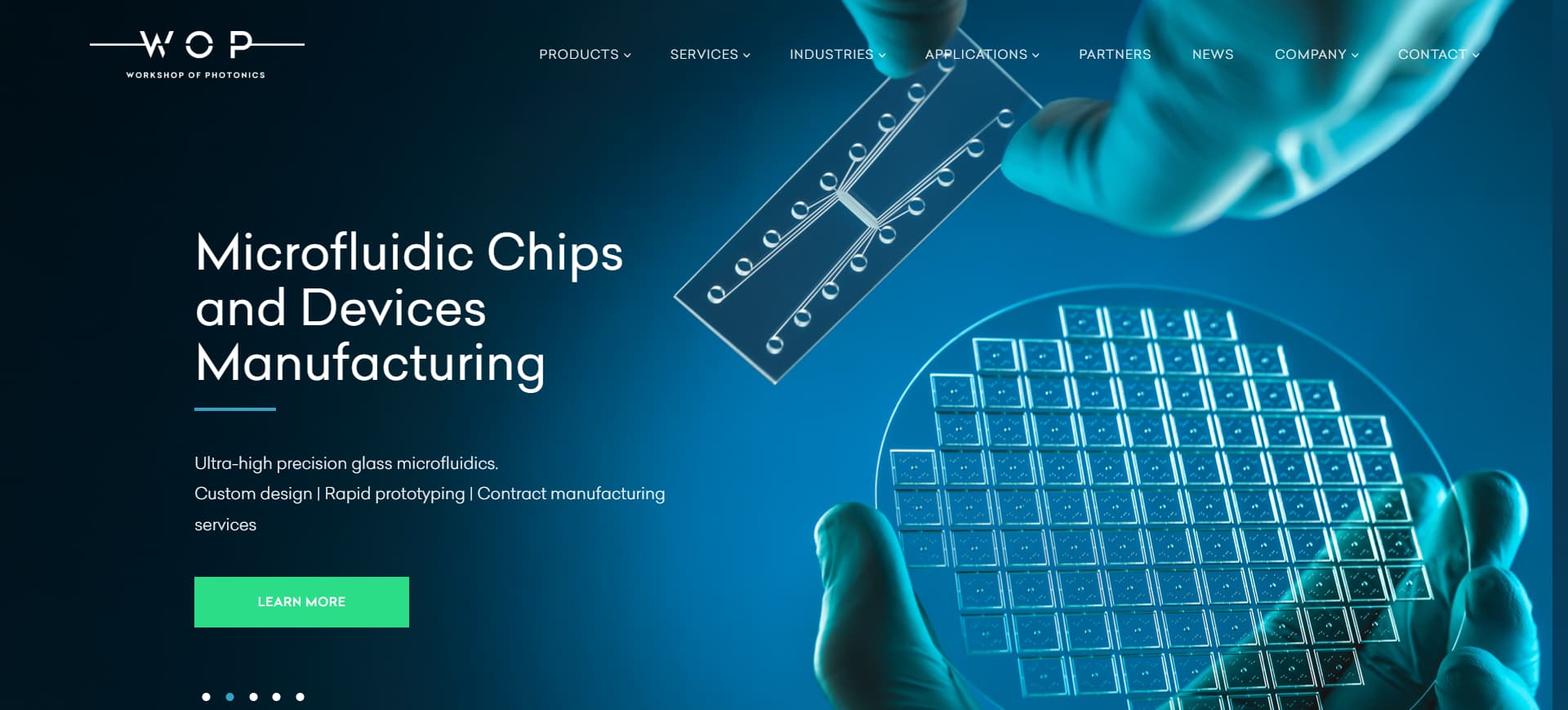
Source: WOP's Official Website (https://wophotonics.com/)
WOP provides microfabrication services for compact devices in fields such as the semiconductor, sensor, and MEMS fields.
This page presents the strengths of WOP's microfabrication services, the materials they can work with, and more.
WOP's microfabrication services
WOP specializes in microfabrication using femtosecond lasers.
This processing technology minimizes thermal impacts while performing high-precision microfabrication at the nano level.
WOP works with a wide range of materials, such as silicon, glass, ceramics, and metal.
Its high-precision processing can be used for glass microfluidic chips, mesh filters with hole diameters as small as 1μm, and more.
One of its features is its integrated support for everything from prototyping to mass production. In particular, it has over two decades of experience* with femtosecond laser microfabrication of glass materials.
* Source: WOP's Website (https://wophotonics.com/)
Fabrication services
WOP performs contactless microfabrication, such as drilling or cutting, at the nano level using femtosecond lasers.
It leverages its expertise in the semiconductor field to provide one-stop services that encompass internal and surface processing of transparent materials and hard, brittle materials. Its diverse services, such as micro-channel formation, optical element 3D structure formation, and micro drilling, have minimal thermal impacts.
Supported materials
WOP handles a wide range of materials, from transparent materials to hard, brittle materials and plastics.
These include glass, sapphire, ruby, silicon, ceramics, polymers, and more.
It can process materials with a high level of optical transparency and can stack and integrate heterogeneous materials.
Supported sizes
WOP has its own cleanroom and can work with substrates measuring up to 300 mm and large glass plates.
It can process microscopic structures with submicron-level (0.1 μm) precision and flexibly work with customers through each phase of research, prototyping, and mass production.
CHECK Finding Your Partner Based on Processing Style
WOP is particularly skilled at femtosecond laser microfabrication of glass material.
It can perform high-precision processing at the nano level with extremely little thermal impact.
It's the perfect partner for companies requiring the internal processing of transparent material, which is difficult to accomplish using conventional mechanical processing, or companies which need to process hard, brittle materials such as glass or sapphire.
In addition to WOP, this site introduces various other microfabrication service providers, categorized by fabrication method, so it's an invaluable resource for anyone trying to decide on a fabrication partner.
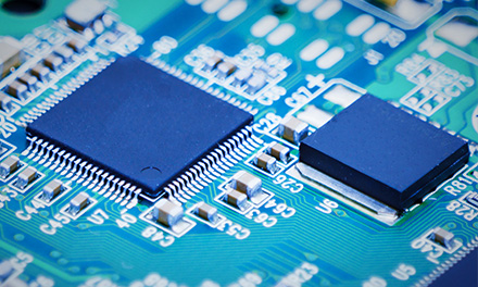
Examples of WOP's microfabrication
Not listed on the company website
Company Information
| Company Name |
Altechna R&D |
| Location |
Mokslininku Street 6A
Vilnius LT-08412
Lithuania |
| Telephone |
+1-(370)-5215-7551 |
| Website |
https://wophotonics.com/ |