Source: TDC Corporation's Official Website (https://mirror-polish.com/en/material_knowledge/tungsten/)
TDC Corporation has posted examples of the polishing it is capable of based on its actual track record of tungsten processing. The first example is of new slit blade production and corrective polishing. The slit blade has a straightness of 0.2 µm and a flatness of 0.1 µm.
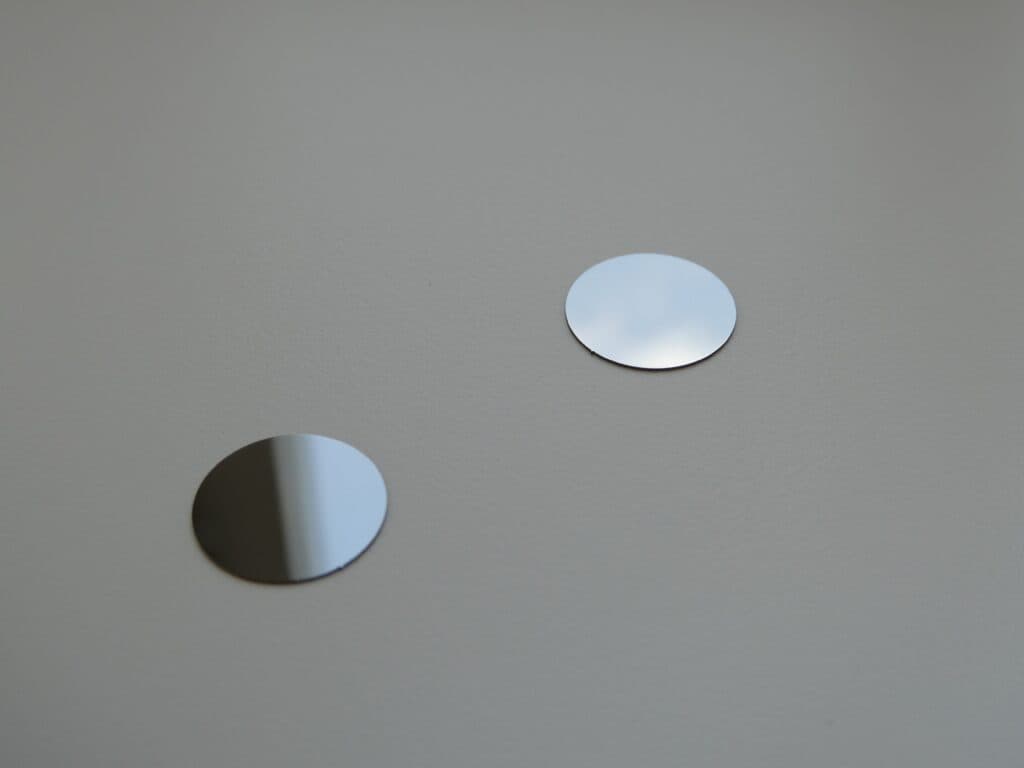
The second example is of a test piece. It was manufactured with a high level of precision, with a surface roughness (Ra), flatness, and parallelism of 0.001 µm.
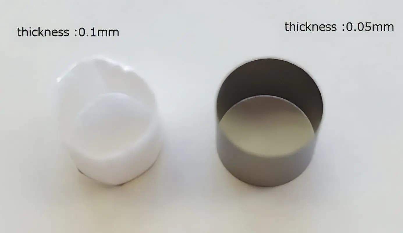
The third example is of the thinning and mirror polishing of tungsten. The 0.05 mm material was thinned to just 0.02 mm and the surface finished to an Ra of 0.001 µm or below.
Research paper: Fabrication of High-Density Microarchitected Tungsten via DLP 3D Printing
High-density microarchitected tungsten was fabricated using digital light processing (DLP). Tungsten ions were dispersed in water-based photoresin and microarchitecture was fabricated through light exposure. Three-step debinding and sintering were used to create dense three-dimensional structures with minimal internal defects.
A minimum feature size of 35 μm and a surface roughness (Ra) of 2.86 μm were achieved.
Among the metals, tungsten has an especially high melting point (approx. 3,700℃)* and it is almost as dense as gold, making it an extremely heavy metal. While it is a very hard metal, it tends to be brittle at room temperatures, making it an extraordinarily difficult-to-cut material. Although it is highly heat resistant, it is susceptible to oxidation at high temperatures.
* Source: PubChem [Melting Point in the Periodic Table of Elements] (https://pubchem.ncbi.nlm.nih.gov/ptable/melting-point/)
Methods for milling tungsten
In lathe machining, materials are spun quickly and a fixed tool called a turning tool bit is used to carve away material to make cylindrical shafts, electrode components, and the like. In milling, a spinning tool such as an end mill is spun and applied to the material to carve away flat surfaces, create grooves, drill holes, or make die components.
In threading, specialized tools such as taps or thread mills are used to carve spiral grooves (screw threads) in the material.
[Choose by Fabrication Type] Top Three Recommended Microfabrication Partners
For difficult-to-cut materials
Koyo High Precision
Source: Koyo High Precision website (https://koyohighprecision.com/)
Examples of supported materials
Tungsten, molybdenum, tantalum,etc.
Main fabrication technologies
Micro drilling
Lathe machining
Milling
Why We Recommend
They perform fabrication for a wide range of sizes, from ⌀3 to 220 mm,and they can handle everything from prototype development to mass production fabrication for difficult-to-cut materials
They can achieve a fabrication precision of ±3 μm even for tungsten,which is known for being difficult to cut.