Boston Micro Fabrication
Open Table of ContentsClose Table of Contents
Source: Boston Micro Fabrication's Official Website (https://bmf3d.com/)
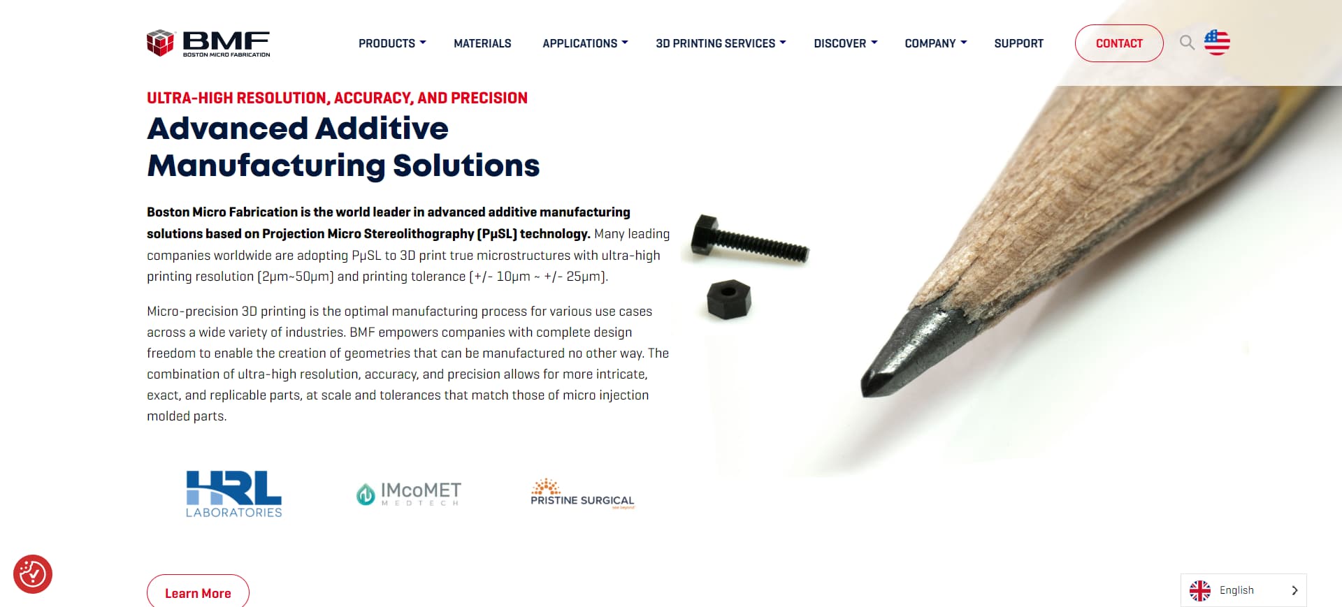
Boston Micro Fabrication provides microstructure 3D printing systems that use photocuring and are capable of 2 µm- and 10 µm-class ultra high resolution on semiconductor substrates.
This page introduces the features of its systems' microfabrication, the processing they can provide, processing examples, and more.
Boston Micro Fabrication's microfabrication systems
Boston Micro Fabrication supplies services using the microArch series of industrial 3D printing systems. These systems are capable of 3D printing structures finer than a human hair.
One of the features of these systems is that they use proprietary PµSL technology.
Ultraviolet light is used to cure liquid resin at the micro level, enabling the free design of microscopic channels, holes, pillars, chip structures, and more.
Boston Micro Fabrication is a manufacturer, so it does not take on ongoing processing requests.
However, as part of the proof of concept (PoC) services it provides in advance of system deployment, it does accept prototype and demo fabrication requests in some regions.
Supported services
The microArch series uses molding materials like photocurable resin and ceramics to create conical, cylindrical, and rectangular column-shaped pin and pillar structures.
These products can also form circular holes, square holes, and three-dimensional shapes such as thin-walled structures.
Supported materials
Boston Micro Fabrication's devices support a unique range of plastics, so customers can select the material with the heat resistance, mechanical strength, flame resistance, biocompatibility, dissolvability (for auxiliary materials and internal structure materials used to support fabrication), and other characteristics that best fit their finished item's intended objectives.
Supported sizes
The sizes that are supported vary by device.
Circular platforms can have diameters of 42 mm to 56 mm and heights of up to 30 mm (M150/M150Pro). Long, thin components up to 90 mm long can be fabricated using microCube T10.
The X axis and T axis can be up to 100 mm (* Specific values will vary depending on the model and processing conditions).
CHECK Finding Your Partner Based on Processing Style
Boston Micro Fabrication's systems can reproduce shapes as small as 2 µm and have exceptional dimensional tolerances. Customers can consult with Boston Micro Fabrication from the design phases of semiconductor-related micro-jigs and complex 3D shapes to improve the efficiency of prototype verification.
This site recommends various microfabrication service providers for companies searching for microfabrication partners.
Case examples of use of Boston Micro Fabrication's microfabrication systems
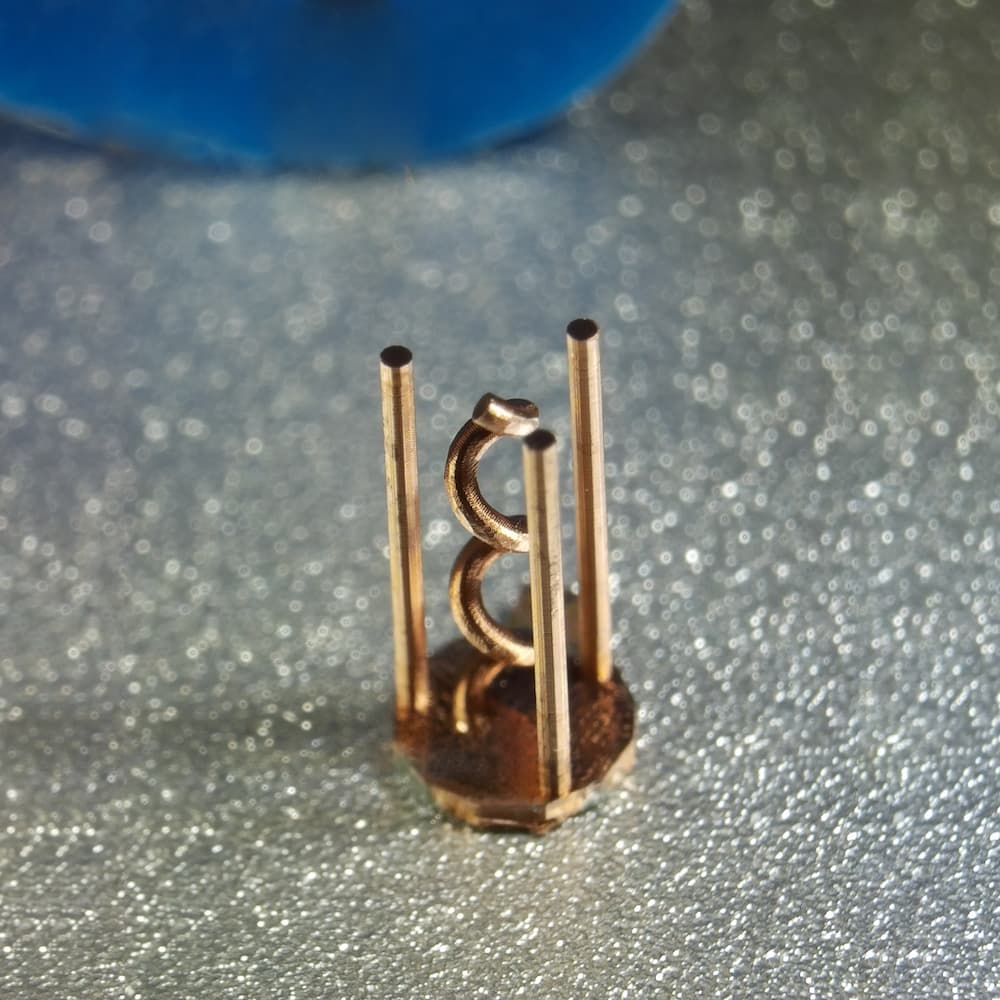
Using 3D printing and metal coating to reduce weight
and improve functionality
Source: Boston Micro Fabrication's Official Website (https://bmf3d.com/resource/next-gen-microfabrication-with-3d-printing-and-coatings/)
A customer is using the microArch S240 (10 µm resolution, layer thicknesses of 10 µm to 40 µm) to combine polymer 3D printing and surface treatment to expand the functionality of components using protective, conductive, metallic coatings.
By combining 3D printing, used for the complex internal structural design, and metallic coating technologies, it has succeeded in reducing the weights of these components to 1/6 of their original weight while maintaining the same performance as conventional metal components.
The technologies are being used to make sensors, electrodes, electrical contacts, and other components more compact and more powerful.
* Source: Boston Micro Fabrication's Official Website (https://bmf3d.com/resource/next-gen-microfabrication-with-3d-printing-and-coatings/)
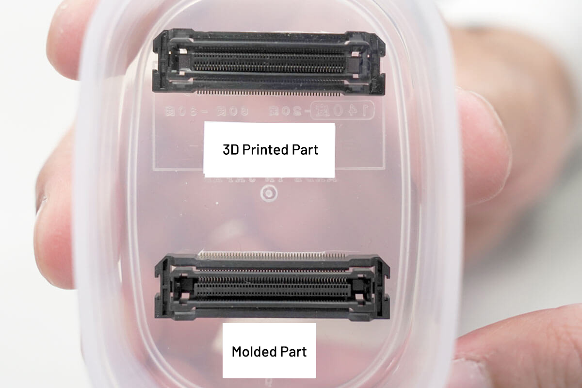
Prototyping electronic circuit connectors with high precision 3D printing
Source: Boston Micro Fabrication's Official Website (https://bmf3d.com/resource/prototyping-electronic-circuit-connectors-with-high-precision-3d-printing/)
Electronic circuits become more compact and use higher frequencies and voltages.
This case example is of a company which was struggling to achieve sufficient accuracy and rapid lead times for ultra-compact connector prototypes measuring just a few mm wide and 1 mm high.
It was using the conventional approach of metal fabrication, so its prototypes sometimes took as long as a month to create.
Thanks to Boston Micro Fabrication's microArch S140 (10 µm resolution), it was able to create components with pinholes spaced 0.4 mm apart that met the requirements of conformance tests.
This enabled the customer to perform iterative prototyping with fast prototyping cycles.
* Source: Boston Micro Fabrication's Official Website (https://bmf3d.com/resource/prototyping-electronic-circuit-connectors-with-high-precision-3d-printing/)
Company Information
| Company Name |
Boston Micro Fabrication |
| Location |
8 Mill & Main Street 310
Maynard, MA 01754
USA |
| Telephone |
+1-(978)-637-2050 |
| Website |
https://bmf3d.com/ |