Atomica
Open Table of ContentsClose Table of Contents
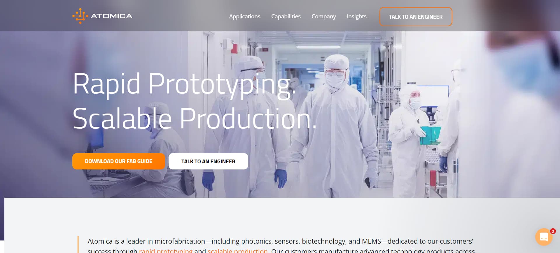
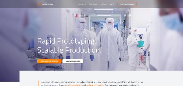
Source: Atomica's Official Website ((https://atomica.com/)
Atomica is an American company that provides micro-precision microfabrication services and mass production services for fields such as the MEMS and photonics fields.
This page presents the strengths of Atomica's microfabrication services, the materials they can work with, and more.
Atomica's microfabrication services
Atomica's strengths lie in etching technologies (DRIE) for materials such as silicon and glass. It uses plasma to perform vertical etching while protecting sidewalls, creating thin, deep, high-precision grooves and holes (with high aspect ratios).
DRIE generally has minimal thermal impact, and the surface produced by etching is smooth, which makes it easy to bond heterogeneous materials. This helps reduce development lead time for MEMS sensors and optical devices.
Atomica performs its processing in a cleanroom whose quality management system has received ISO 9001 (international standard) certification. It is also registered under the US Department of Defense's International Traffic in Arms Regulations (ITAR) (as of November 2025*).
* Source: Atomica's Website (https://atomica.com/capabilities/)
Fabrication services
Atomica has an in-house system that covers all of the processes involved in MEMS manufacturing.
It handles everything from creating microscopic patterns using photolithography to removing unnecessary portions using etching and three-dimensional structure creation using plating and bonding.
Supported materials
Atomica works with materials such as silicon, SOI, glass, quartz, and III-V, and can stack and fuse heterogeneous materials that typical MEMS fabs struggle with.
It also provides plating services, so it can form high-profile components (molds, conductive coils, magnets, actuators, etc.).
Supported sizes
Atomica has a roughly 2,800 m2 cleanroom and works with both 6-inch (approx. 152 mm) and 8-inch (approx. 203 mm) wafer substrates.
CHECK Finding Your Partner Based on Processing Style
One of Atomica's strengths is that it combines multiple microfabrication technologies, focusing on DRIE, to perform both microfabrication of micro-scale components and large-scale production.
It is a great partner for companies developing and mass-producing high performance, highly complex devices requiring the stacking of heterogeneous materials, MEMS integration, photonics structures, and the like.
In addition to Atomica, this site introduces various other microfabrication service providers, categorized by fabrication method, making it an invaluable resource for anyone trying to decide on a fabrication partner.
Examples of Atomica's microfabrication
Not listed on the official website
Company Information
| Company Name |
Atomica Corp. |
| Location |
75 Robin Hill Road
Goleta, CA 93117
USA |
| Telephone |
+1-(805)-364-2266 |
| Website |
https://atomica.com/ |