Citrogene
Open Table of ContentsClose Table of Contents
Source: Citrogene's Official Website (https://www.citrogene.com/)
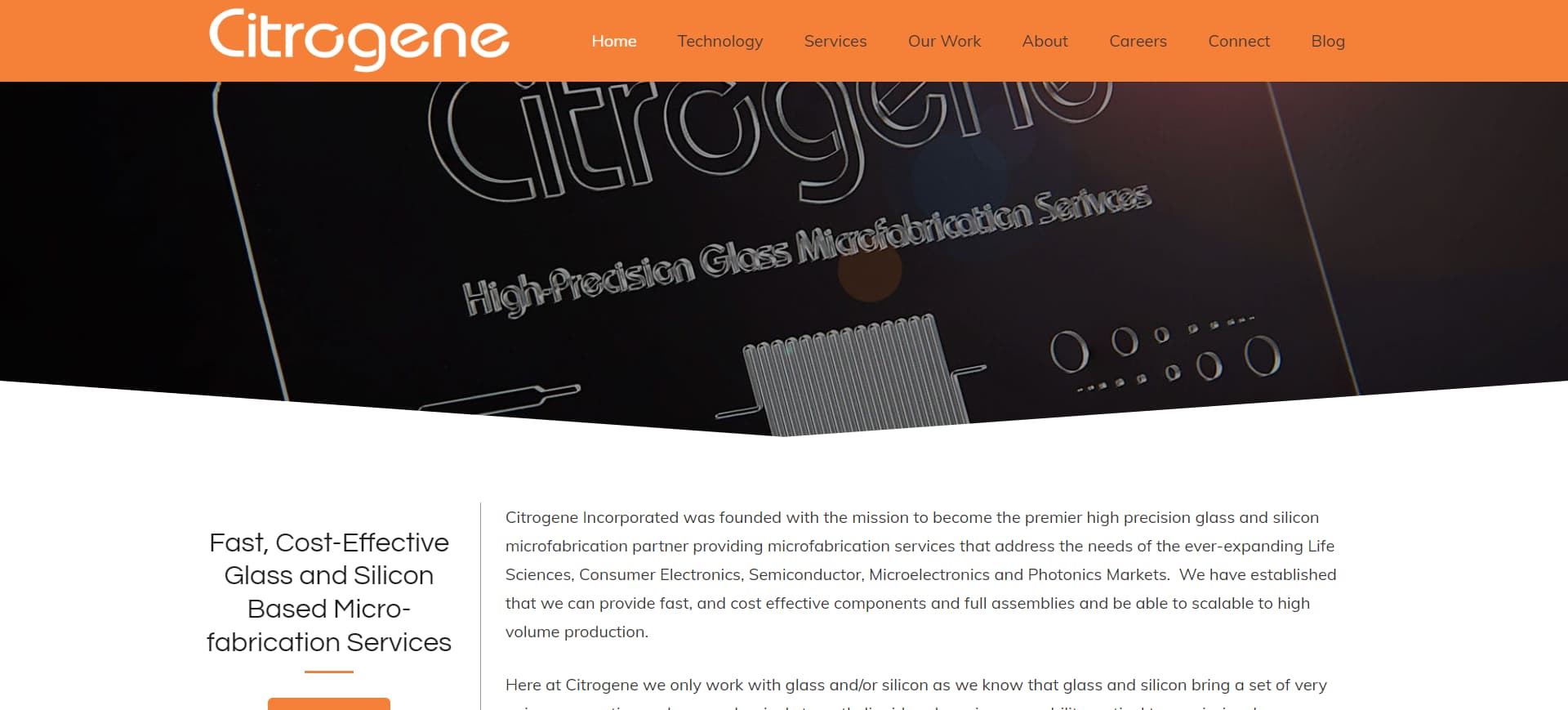
Citrogene is an American company that provides high-precision laser microfabrication services for a wide range of glass materials.
This page presents the strengths of Citrogene's microfabrication services, the materials they can work with, and more.
Citrogene's microfabrication services
Citrogene uses its proprietary laser microfabrication technologies to form channels between 30 µm and 200 µm (0.03 mm and 0.20 mm) and to drill through holes with diameters of 25 µm (0.025 mm) in hard glass. It performs high-precision microfabrication of channels and holes with a minimum pitch of just 100 µm 0.10 mm).
Citrogene's technologies have little thermal impacts and avoid surface damage or cracking, so they're well-suited for microchannel chips with delicate structures.
For example, they can be used to create minute channels, through holes, and electrode patterns with a high degree of reproducibility for fields such as the biochip or lab-on-a-chip devices.
Fabrication services
Citrogene's contactless laser microfabrication offers a greater degree of shape freedom and shorter turnaround than conventional drilling or photolithography.
It provides a wide range of services, including drilling, cutting, channel formation, surface processing, and more.
Supported materials
Citrogene primarily works with glass materials such as quartz, fused silica, BOROFLOAT, and alkali-free boroaluminosilicate, which have little thermal expansion.
It also works with inexpensive, easy-to-process glass materials such as soda lime and strong, scratch-resistant aluminosilicate.
Supported sizes
Citrogene can work with glass wafer substrates with diameters between 15 mm and 300 mm and thicknesses between 0.03 mm and 3.0 mm.
CHECK Finding Your Partner Based on Processing Style
Citrogene uses proprietary technologies to perform processing on glass using ultra-short pulses, without generating heat. This minimizes heat effects and prevents cracking and chipping.
It's highly suited to development projects for medical/analysis chips, optical sensors, microfluidic devices, and other devices that require precise structures while maintaining the transparency of glass.
In addition to Citrogene, this site introduces various other microfabrication service providers, categorized by fabrication method. Use it to find the fabrication partner that's right for you.
Examples of Citrogene's microfabrication
Not listed on the official website
Company Information
| Company Name |
Citrogene Incorporated |
| Location |
2528 Qume Drive, Suite 6
San Jose, CA 95131
USA |
| Telephone |
+1-(408)-930-5070 |
| Website |
https://www.citrogene.com/ |