HRL Laboratories
Open Table of ContentsClose Table of Contents
Source: HRL Laboratories's Official Website (https://www.hrl.com/products-services/foundry)
HRL Laboratories was established as Hughes Research Laboratories in 1948, and became a limited liability company (LLC) in 1997.
For over 70 years, it has been conducting research and development in the semiconductor and microsystem fields.
This page introduces its microfabrication features, the processing services it offers, processing examples, and more.
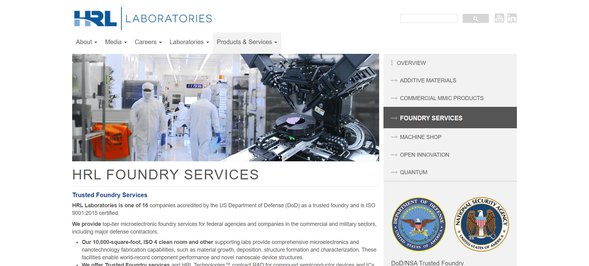
HRL Laboratories' microfabrication services
HRL Laboratories offers microfabrication services through its Microfabrication Technology Laboratory (MTL) division.
It has a 10,000 square-foot ISO Class 4 cleanroom and has been certified as a Category 1A Trusted Foundry by both the US Department of Defense and the NSA.*
It is ISO9001- and AS9100-certified and its quality management system also encompasses semiconductor-related processes.
It can handle all processes, from epitaxial growth to thin-film deposition, pattern formation, etching, post-processing, and evaluation, entirely in-house.
HRL Laboratories offers comprehensive services including prototype manufacturing, pilot production, and material evaluation.
* Source: HRL Laboratories (https://www.hrl.com/laboratories/mtl)
Fabrication services
HRL Laboratories integrates multiple processing methods for each processing stage.
First, epitaxial growth technologies (MBE/MOCVD) are used to form high quality crystal layers on substrates. Then electron beam deposition and sputtering are performed to form thin films.
Following this, patterns are transferred to workpieces using photolithography and electron beam lithography. Wet/dry etching and ion milling are used to fabricate nanoscale structures.
Chemical mechanical polishing (CMP), bonding, dicing, and other post-processing are then performed.
This processing approach enables HRL Laboratories to manufacture compound devices made of heterogeneous materials and prototypes with multi-layer structures.
Supported materials
HRL Laboratories can work with a wide range of materials, such as metals, composite metals, dielectrics, polymers, and quartz, primarily focusing on III-N and III-As/Sb compound semiconductors.
In its thin-film deposition, it has already established film conditions for over 50 different types of metals and dielectric materials.
It can also flexibly accommodate new materials and perform experimental composition verification.
Supported sizes
HRL Laboratories has automatic photolithography transport systems for 3-inch and 4-inch substrates, and uses manual handling for substrates measuring larger than 4 inches and for partial pieces.
CHECK Finding Your Partner Based on Processing Style
HRL Laboratories' strengths lie in its microfabrication for cutting-edge devices, focusing on compound semiconductors.
From material growth to post-processing and evaluation, HRL Laboratories handles everything in-house.
One of its distinctive features is the flexibility of its contract and intellectual property agreements.
It makes a great partner for semiconductor and aerospace companies who need high reliability.
This site recommends various microfabrication service providers for companies searching for microfabrication partners.
Examples of HRL Laboratories' microfabrication
Not listed on the company website
Company Information
| Company Name |
HRL Laboratories, LLC |
| Location |
3011 Malibu Canyon Road
Malibu, CA 90265
USA |
| Telephone |
+1-(310)-317-5000 |
| Website |
https://www.hrl.com/ |