Protolabs
Open Table of ContentsClose Table of Contents
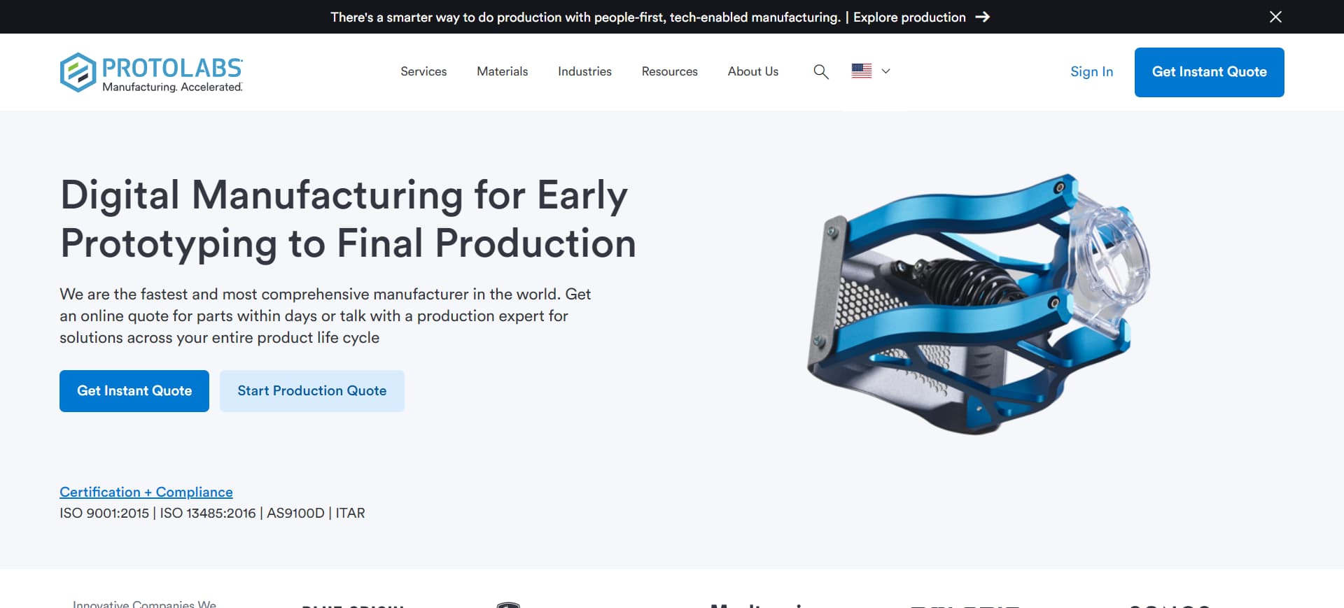
Source: Protolabs's Official Website (https://www.protolabs.com/)
Protolabs supports multiple fabrication methods for plastic and metal, such as 3D printing, CNC cutting, and injection molding.
This page introduces its microfabrication features, the processing services it offers, processing examples, and more.
Protolabs' microfabrication services
Compact, fast, and accurate.
These are at the heart of Protolabs' operations, shared in common by its various processing methods.
One of its features is the use of MicroFine (Protolabs' own proprietary high-precision stereolithography material) in its varied stereolithography (SLA) processing methods to provide completely digital on-demand manufacturing services, from prototyping to small lot production.
Unlike conventional processing-on-consignment, it handles the entire process, from project estimate creation to manufacturing, simply by uploading CAD data online.
This makes it a great choice for prototype development in the semiconductor or electronic component fields, where development speed is critical.
Fabrication services
Protolabs offers both additive services, which are great for reproducing complex, minute shapes, and subtractive services, whose strengths lie in dimensional precision and surface quality.
The additive approach can be used to create microfluidic chips and prototypes with complex internal structures, while the subtractive approach is suited to high-precision processing of metal and plastic components.
Supported materials
Protolabs can work with plastics such as ABS-like resin for SLA, nylon, and various photopolymers.
It has a selection of commercial-grade materials suited for everything from prototypes to small-lot production.
Supported sizes
In its MicroFine processing, Protolabs can reproduce shapes with a pitch of 0.025 mm per layer and details as small as 0.07 mm (fine shapes).
Its CNC machining maintains a dimensional tolerance of ±0.02 mm, and it can perform cutting of fine shapes such as holes and grooves with diameters as small as 0.5 mm.
CHECK Finding Your Partner Based on Processing Style
While Protolabs does not provide semiconductor manufacturing processes such as silicon wafer or thin-film formation, it excels at prototyping and small lot production of peripheral components with find structures, such as microfluidic chips, resin and metal packages, and precision jigs used inside devices.
This site recommends various microfabrication service providers for companies searching for microfabrication partners.
Examples of Protolabs' microfabrication
Not listed on the company website
Company Information
| Company Name |
Proto Labs, Inc. |
| Location |
5540 Pioneer Creek Drive
Maple Plain, MN 55359
USA |
| Telephone |
1-(877)-479-3680 |
| Website |
https://www.protolabs.com/ |