Sharretts Plating Company
Open Table of ContentsClose Table of Contents
Source: Sharretts Plating Company's Official Website (https://www.sharrettsplating.com/)
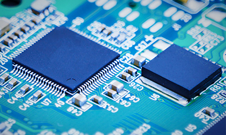
Sharretts Plating Company supplies microfabrication services that utilize photolithography, etching, and other technologies to assist with the processes involved in MEMS manufacturing.
This page introduces its microfabrication features, the processing services it offers, processing examples, and more.
Sharretts Plating Company's microfabrication services
Sharretts Plating Company uses technologies that utilize light to create fine patterns on silicon substrates (photolithography) and technologies that utilize patterns to remove unnecessary material (etching).
Both of these microfabrication technologies are vital for manufacturing semiconductors and MEMS.
Furthermore, it combines these technologies with its surface treatment technologies (such as technologies for forming thin metal layers), which it has developed through its metal surface treatment business, to help create and improve the functionality of the microstructures necessary for electronic and semiconductor devices.
Fabrication services
One of Sharretts Plating Company's features is its use of processing technologies like photolithography and etching.
Specifically, it uses technologies such as bulk micromanufacturing for making internal structures in silicon substrates and surface micromanufacturing for stacking structures on the surfaces of silicon substrates.
By combining these two techniques, it can realize diverse structural designs for microsensors, microdevices, and the like.
Supported materials
Not listed on the company website
Supported sizes
Not listed on the company website
CHECK Finding Your Partner Based on Processing Style
Sharretts Plating Company can handle all microfabrication processes such as the microstructure formation, metal layer formation, prototype development, and other processes involved in MEMS device development, through its integrated system.
That makes it the perfect partner for companies developing MEMS and microdevices.
This site recommends various microfabrication service providers for companies seeking microfabrication partners.
Examples of Sharretts Plating Company's microfabrication
Not listed on the company website
Company Information
| Company Name |
Sharretts Plating Company, Inc. |
| Location |
3315 Connelly Road
Emigsville, PA 17318
USA |
| Telephone |
+1-(717)-767-6702 |
| Website |
https://www.sharrettsplating.com/ |