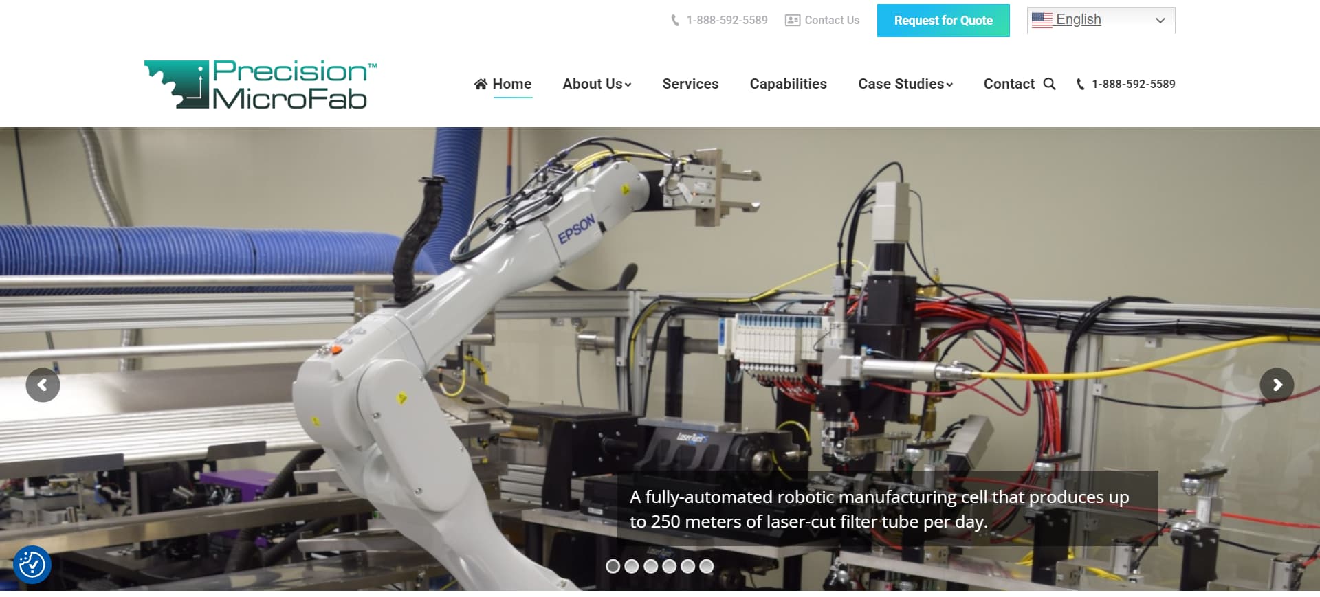
Precision MicroFab
Open Table of ContentsClose Table of Contents
Source: Precision MicroFab's Official Website (https://www.precisionmicrofab.com/)
Precision MicroFab performs micromanufacturing, with a focus on laser processing, to handle orders for diverse microfabrication, including drilling, cutting, welding, ablation, and micromilling.
This page introduces its microfabrication features, the processing services it offers, processing examples, and more.
Precision MicroFab's microfabrication services
One of Precision MicroFab's features is that it has a range of lasers with various bandwidths, which it selects from to match the right laser to the right material.
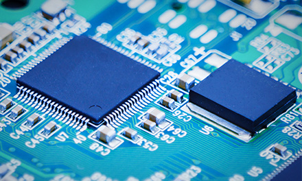
For semiconductors, electronic components, transparent materials, and biomaterials, it uses UV lasers with short wavelengths to perform photoablation.
Photoablation breaks down and removes material with the energy from light, so it produces almost no heat melting or burning.
For materials unsuited to photoablation, such as thicker materials and metals, it instead performs photothermal processing using IR lasers with long wavelengths.
This technology converts light into thermal energy to vaporize and melt materials, so it is well-suited to deep cutting and precision welding.
After processing, it rigorously checks that completed articles meet their requirements and issues inspection reports.
It is has received both ISO 9001:2015 and ISO 13485:2016 certifications, so customers can rely on its quality management system.
Fabrication services
Precision MicroFab uses contactless lasers in a variety of processing techniques.
It can drill holes (both blind holes and through holes) with diameters of less than 1 µm.
In its welding, it keeps weld widths as small as 0.025 mm.
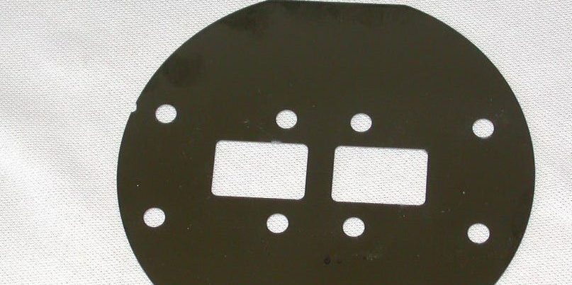
It also offers microfabrication services such as cutting, selective removal, channel machining, and three-dimensional structure fabrication.
Supported materials
Precision MicroFab has made it its policy to support every type of material.
It has processing track records with diverse materials such as metal, glass, ceramics, and polymers.
It can even work with diverse alloys such as alloys with high melting points and difficult-to-cut materials.
Supported sizes
Not listed on the company website.
CHECK Finding Your Partner Based on Processing Style
Precision MicroFab customers enjoy a great deal of freedom in selecting materials.
The company's quality management system meets the exacting standards of industries such as the medical, electronics, and space industries, which have strict regulations and require high levels of reliability. It can serve as a powerful partner to companies which want a single company to meet their varied microfabrication technology needs, such as micro-channel formation, selective film removal, or microwelding.
This site recommends various microfabrication service providers for companies seeking microfabrication partners.
Examples of Precision MicroFab's microfabrication
Precision silicon wafer cutting using infrared lasers
Source: Precision MicroFab's Official Website (https://www.precisionmicrofab.com/casestudies/silicon-wafer-cutting/)
Precision MicroFab has used infrared fiber lasers to machine irregular shapes in silicon wafers with high edge quality.
It adjusted the settings to minimize kerf width, chipping, and spalding, producing sharp cutting faces with knife-edge precision.
This edge quality is of such high precision that this processing can also be used for the fabrication of precision electronic components such as MEMS or silicon devices.
* Source: Precision MicroFab's Official Website (https://www.precisionmicrofab.com/casestudies/silicon-wafer-cutting/)
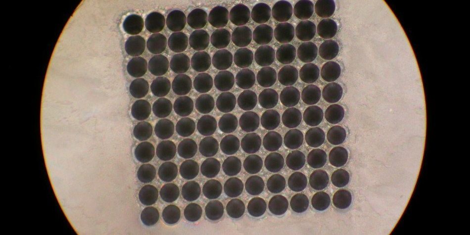
ArF excimer laser micro drilling through 500 µm-thick borosilicate glass
Source: Precision MicroFab's Official Website (https://www.precisionmicrofab.com/micro-drilling-glass/)
Precision MicroFab used a 193 nm wavelength ArF excimer laser to drill a hole array in a 500 µm-thick piece of borosilicate glass.
The hole depths were adjusted by changing the number of laser pulses in stages, with the laser breaking through the glass at 4,500 pulses. The holes in the array are extremely tightly spaced, but there is no cracking or shattering in the walls between them.
Precision MicroFab avoided the problems presented by the highly breakable nature of glass and created a hole array with the high density and high uniformity required by analysis devices and flow control components.
* Source: Precision MicroFab's Official Website (https://www.precisionmicrofab.com/casestudies/micro-drilling-glass/)
Company Information
| Company Name |
Precision MicroFab LLC |
| Location |
7500 Energy Court, Suite 4
Curtis Bay, MD 21226
USA |
| Telephone |
*1-(888)-592-5589 |
| Website |
https://www.precisionmicrofab.com/ |