Teledyne MEMS
Open Table of ContentsClose Table of Contents
Source: Teledyne MEMS's Official Website (https://www.teledynemems.com/)
Teledyne MEMS supplies the semiconductor field with microfabrication services for silicon, glass, and other materials.
This page presents the strengths of Teledyne MEMS's microfabrication services, the materials they can work with, and more.
Teledyne MEMS's microfabrication services
Teledyne MEMS's core services are 5x lithography services using ASML photolithography equipment.
Its strengths include its pattern resolution capabilities, capable of creating features measuring just 0.35 µm (0.00035 mm), and its positioning accuracy of ±0.1 µm (±0.0001 mm).
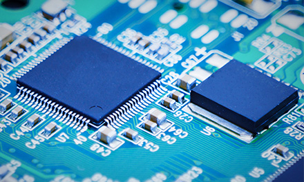
These processes are used for a wide range of applications, such as medical MEMS (pressure sensors, flow sensors, etc.), optical MEMS (micromirrors, optical shutters, etc.), inertia sensors, biochips, and microchannel devices.
Fabrication services
Teledyne MEMS's fabrication services are primarily centered on photolithography, printing the circuit patterns used in semiconductors.
It also offers etching to remove unnecessary portions, processing methods for depositing films on substrates based on item usage purposes, and the drilling of microholes for wiring, all in-house.
Supported materials
Teledyne MEMS works with diverse wafer materials, such as silicon, polymer, and glass.
It supports the manufacturing of devices for a wide range of fields, including the optical, medical, bio MEMS, and pressure sensor fields.
Supported sizes
Teledyne MEMS manufactures MEMS with its 150 mm and 200 mm wafer lines.
The lines have a high degree of commonality, so processes set up on the 150 mm line can be transferred to the 200 mm line.
The 200 mm line also supports wafer-level bonding, integrating MEMS structures and CMOS circuits.
CHECK Finding Your Partner Based on Processing Style
Teledyne MEMS excels at all kinds of surface processing used in the manufacturing of MEMS.
It therefore makes a great partner for companies developing MEMS sensors, optical devices, and semiconductor processes, which require micron-level pattern formation and multilayer film structures.
In addition to Teledyne MEMS, this site introduces various other microfabrication service providers, categorized by fabrication method.
It's an invaluable resource for companies trying to decide on a fabrication partner.
Examples of Teledyne MEMS's microfabrication
Not listed on the official website
Company Information
| Company Name |
Teledyne Technologies Incorporated |
| Location |
1049 Camino Dos Rios
Thousand Oaks, CA 91360
USA |
| Telephone |
+1-(805)-373-4545 |
| Website |
https://www.teledyne.com/ |