Hawk Semiconductor
Open Table of ContentsClose Table of Contents
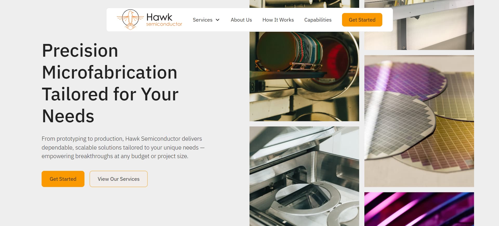
Source: Hawk Semiconductor's Official Website (https://www.hawksemiconductor.com/)
Hawk Semiconductor manufactures semiconductors and MEMS devices using materials such as silicon and metal.
It also provides flexible material processing services for articles such as microfluidic chips using PDMS casting.
This page introduces its microfabrication features, the processing services it offers, processing examples, and more.
Hawk Semiconductor's microfabrication services
Hawk Semiconductor is a one-stop provider of everything from product concept design to strategy design, processing, manufacturing, and verification.
Each processing stage is monitored and controlled in real time.
Product quality is assured through FE-SEM, AFM, and other verification, and the company issues both processing records and quality reports.
There are no minimum lot sizes, so Hawk Semiconductor can even flexibly work with customers during the research and development phase.
Fabrication services
Hawk Semiconductor uses i-line 5x stepper and ebeam lithography systems for submicron resolution, and mounts devices with technologies such as backside alignment and multi-layer processing.
For etching, customers can choose dry etching techniques like DRIE and plasma etching or wet etching techniques matched to the characteristics of their materials.
It supports both isotropic and anisotropic profiles.
Supported materials
Hawk Semiconductor works with not only typical semiconductor materials like oxide films and metal films but also other major film materials such as silicon dioxide, titanium dioxide, metal, aluminum, and platinum.
Supported sizes
Hawk Semiconductor can perform photolithography for wafers measuring up to 150 mm.
CHECK Finding Your Partner Based on Processing Style
Hawk Semiconductor has no minimum lot size restrictions, and it offerssub-micron resolution photolithography, wide range of film deposition methods, etching (including DRIE), measurement, and packaging services.
It also enables customers to begin working with PDMS and flexible devices, so it's a perfect partner for companies interested in research and development or small lot production with custom specifications.
This site recommends various microfabrication service providers for companies seeking microfabrication partners.
Examples of Hawk Semiconductor's microfabrication
Not listed on the company website.
Company Information
| Company Name |
Hawk Semiconductor |
| Location |
4108 Spring Lake Boulevard
Ann Arbor, MI 48108
USA |
| Telephone |
+1-(231)-740-2720 |
| Website |
https://www.hawksemiconductor.com/ |